What is Field Effect Transistor:
Field effect transistor is a unipolar device. Meaning is current conduction takes place only due to one type of carrier electron or holes.
This is the major difference between the bipolar junction transistor and field effect transistor.
BJT takes the conduction in electron and holes.
Here we are going to see only field effect transistor
The FET is of two types they are junction field effect transistor and metal oxide field effect transistor.
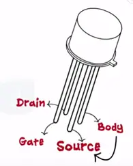
JFET was first introduced by Shockley in 1952. JFET is a four terminal device gate, drain and source fourth terminal called as body terminal always connected to the source.
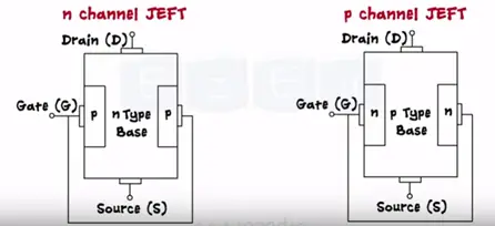
JFET is of two types N-channel and P-channel. Thus we represent only three terminals in the symbol; of JFET.
Construction of N channel JFET (Junction Field Effect Transistor)
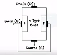
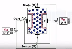
The name N channel signifies that electrons are the majority charge carriers. To form the N channel JFET take N type semiconductor as a base and dope it with P type semiconductor at both ends. Both these P regions are electrically connected to each other and only contact in taken out which is called as Gate (G). Two more terminals are taken out in N substrate and are called as source and drain.
JFET has three terminals source, drain and gate similar to BJT JFET also has two PN junctions.
Construction P channel JFET
Take P type as a substrate and dope it with N type semiconductor at both ends to form the gate.
Working of JFET & Biasing of JFET
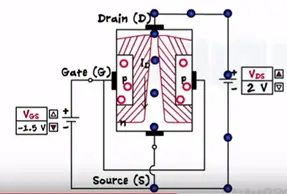
With the two voltage sources one between the gate and source as Vgs and second between the drain and source as Vds the source acts a common terminal. Initial when no volt is applied the depletion is formed across the two junctions. Being on N type the drain to source channel contains as majority charge carriers.
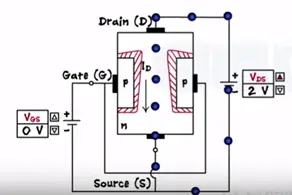
Application to small drain to source voltage these makes electron flow from the source to drain as the positive voltage at the drain attacks them. Thus the drain current flows through the JFET from drain to the source.
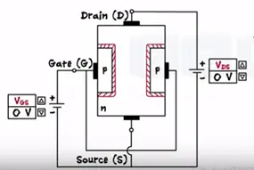
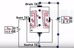
Let’s keep the Vds constant and apply some gate to source voltage as Vgs=0.5 V.
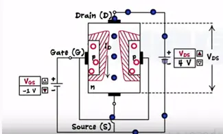
P region contains volts applying negative voltage the gate makes the PN junction reverse biased.
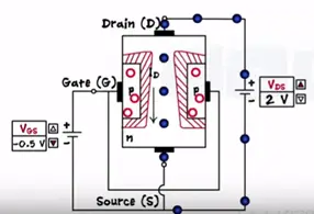
The depletion region width increases and it penetrates deeply into the channel. Decreasing the channel width the drain current reduces.
Now if we increase the gate voltage towards the more negative side the depletion region goes increasing and point channel get depleted completely the value Vgs is called pinch off voltage or threshold voltage at this point current flow stops.
Now let’s keep Vgs constant between zero volts and the pinch value increases the Vds voltage (0<Vgs<Vpinchoff). Vds is nothing but voltage across the channel increases as remove towards the drain.
And also reverse bias voltage of Vgs is the highest at the drain. Thus the depletion region gets the trapped shape near the drain Vds=10 V and channel become much narrower.
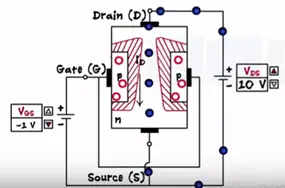
Thus Id remains constant characteristics graph become non-linear.
Why Vgs is not positive?
Gate voltage primary controls the flow of the drain current. If we apply Vgs positive this will make Vgs= positive.
PN junction forward bias and gate control current flow. Thus we never apply voltage 0 volts to gate terminal Vgs<0.
The JFET output current Id controlled by the input current Vgs. Thus FET is voltage controlled device. BJT is current controlled device.
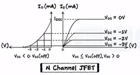
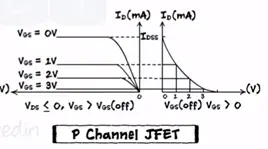
Characteristics of JFET (Junction Field Effect Transistor)
Application of Field Effect Transistor
- High input impedance
- Voltage controlled device
- It provides high degree of isolation between the input and output.
- Less noisy


