Transistor Working Principle:
Transistor is nothing but a transferred resistor (Transistor = transferred + resistor). An anti-parallel diode is called transistor, which means two diodes are connected reversely to form a new electronics component, such components are called Transistor. They are acts as switch. It is one of the active components. It does not obey ohms’ law.
However, they have two types according to the flow of charge carriers. One is BJT (Bipolar Junction Transistor); in that the current flow is due to both majority and minority carriers, whereas in FET (Field Effect Transistor), the current flows due to majority carriers. Also BJT is divided in to two types according to the diode connection. Two types of BJTs
- NPN Transistor
- PNP Transistor
In this article we are going to talk about NPN Transistor.
NPN Transistor:
Two anti-parallel diodes jointly create a NPN Transistor, which means NP+PN = NPN Transistor. Finally, we get Three Terminal Such as Collector (C), emitter (E) and Base (B) terminals. In our NPN transistor, the emitter terminal is heavily doped and it emits the electrons, Base terminal lightly doped and Collector terminal doped intermediate between other two.
Terminal Notations:
Emitter => Emits the electrons
Collector => Collects the electrons for NPN (for PNP it collects the holes)
Holes means => Positive charges.
Collector is a largest region as compared with emitter and base region.
Let’s we take common base mode of NPN Transistor.
Note: Common base mode means; the common terminal of the transistor is considering as base terminal.
Transistor Working Principle:
Before understanding about Transistor working principle, You should know the meaning of the following region in the transistor. They are emitter region, forward barrier region, base region, reverse barrier region, and collector region.
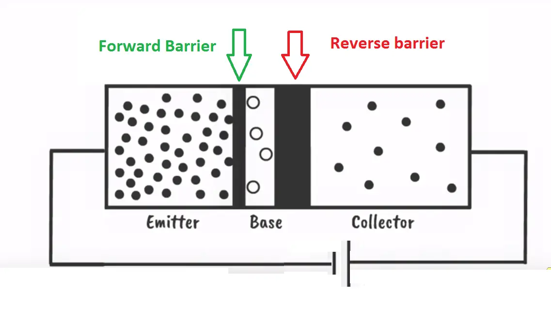
Emitter Region: heavily doped, N type semi-conductor, High Number of free electrons, Intermediate size.
Forward barrier region: The region between base and emitter. This region is formed due to the attraction of holes in the base region and electrons in the emitter region, finally it creates an internal electric field and the value will be around 0.7 Volts for silicon semiconductor and 0.3 for germanium conductor. It is also called Junction J1.
Note: To break this barrier, we should apply source voltage is more than the barrier voltage. I.e for silicon the applied voltage should be more than 0.7Volts. Then only the current starts flowing.
Base Region: lightly doped, P type semiconductor. Few number of holes, very small size, typically few micro meters
Reverse barrier region: It is formed due to the base and emitter reverse bias and the resistance of in this barrier is infinity. It is also called junction J2
Collector region: Intermediate doped (wider range), N type semiconductor, Intermediate number of free electrons. Bigger size as compare to all other region. Typically, it will be few millimeters.
Doping Level of the NPN transistor will be emitter > collector > base.
Region Size will be collector > emitter > base.
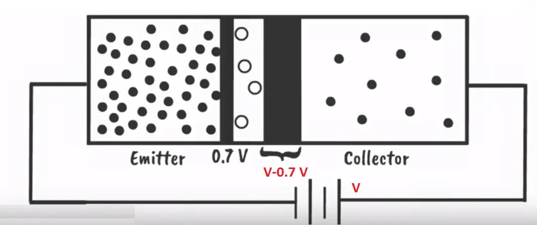
First, Now Take a common emitter configuration, now apply a small voltage (V) across collector (+ve) and emitter (-ve) terminal. Here the 0.7 volts will be dropped at forward potential barrier and remaining voltage (V-0.7 volts) will be dropped at reverse barrier region. Because reverse barrier has infinity resistance. Therefore, the net current flow through the transistor is zero. Hence the transistor act as open switch.
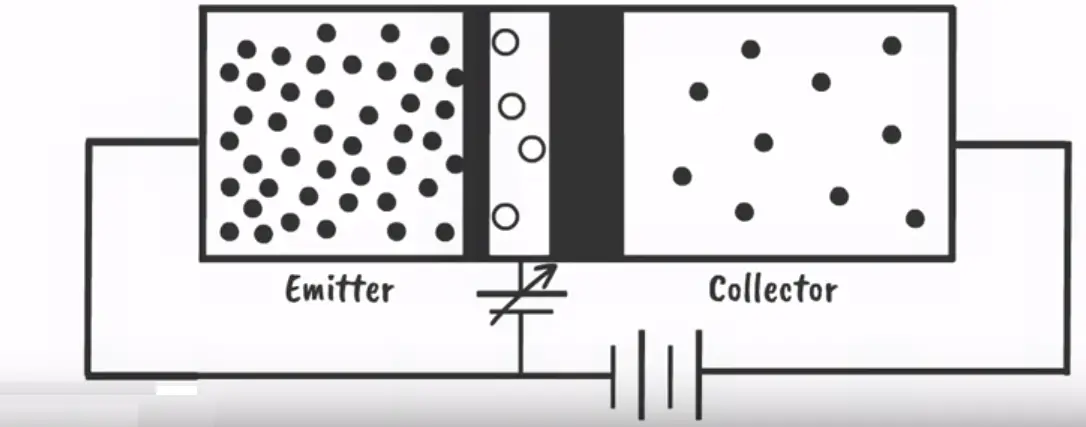
Now additionally, we apply a small potential difference across the base terminal (+ve) to emitter (-ve) terminal, which means base and emitter terminal become forward bias and collector and base become reverse bias. Now due to heavy doped emitter region, the electrons tries to recombine with the base region’s hole by crossing Junction J1. Since electrons starts moving from emitter to base.
Because of we already applied electric field across the junction J1. At the same time due to smaller region, only few number of electrons recombine with the holes in the base region, therefore the electron enters into the collector region by crossing J2 junction (reverse barrier). As there is a reverse barrier present across the base-collector junction, it will not stop the flow of free electrons from the base to the collector as the free electrons in the base region are minority carriers.
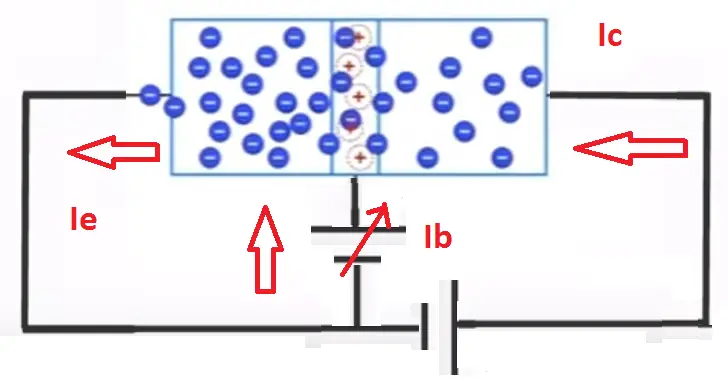
Consider Ib as Base current, Ic as collector current and Ie as emitter current..In CE configuration..
Ie=Ib+Ic
Finally, electron stats flow through the emitter to collector region. At the same time, due to the combination of holes and electrons in the base region causes a small amount of current flows through the base to emitter region. Its typically 2 to 5 % of the collector to emitter current. It is called base current.
Now we increase the base voltage, In this situation due to increased forward voltage across emitter-base junction proportionately more free electrons will come from the emitter region to the base region with more kinetic energy. This causes a proportionate increase of collector current. In this way, by controlling small base signal, we can control quite a large collector signal. This is the basic working principle of transistor.

