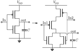
Q.26 Transistor geometries in a CMOS inverter have been adjusted to meet the requirement for worst case charge and discharge times for driving a load capacitor C . This design is to be converted to that of a NOR circuit in the same
technology, so that its worst case charge and discharge times while driving the same capacitor are similar. The channel length of all transistors is to be kept unchanged. Which one of the following statements is correct?
(A) Widths of PMOS transistors should be doubled, while widths of NMOS transistors should be halved.
(B) Widths of PMOS transistors should be doubled, while widths of NMOS transistors should not be changed.
(C) Widths of PMOS transistors should be halved, while widths of NMOS transistors should not be changed.
(D) Widths of PMOS transistors should be unchanged, while widths of NMOS transistors should be halved.
Answer: (B)
Explanation:


