DIODES
The William henry Ecdes was first formed the diode in 1919. It is derived from greek roots from DI- two and ODE- electrode.
The different types of diodes are LED used in street lights LEDs, photo diodes used in light detectors or in light sensors in industries like communication, head lights of the cars etc.
PN junction diode acts a base for all above diodes are modified form the PN junction diode.
Construction of PN junction diode
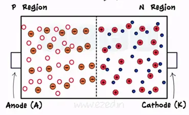
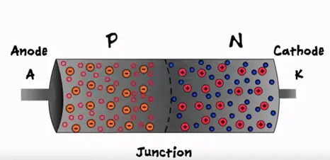
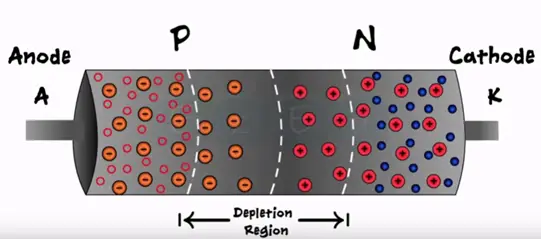
Here in a name PN junction diode itself suggest P for P-region and N for N-region for pure semiconductor material.
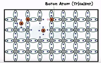
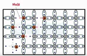
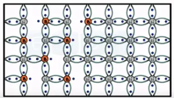
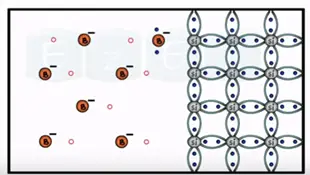
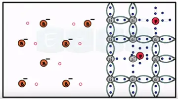
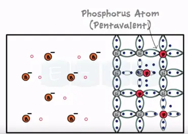
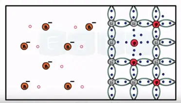
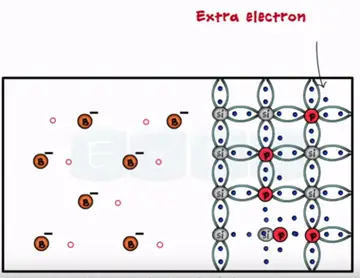
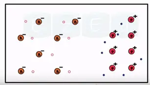
We dope P-type impurities like boron in the left half of one slice. Boron in the trivalent accepts one electron from the neighbouring silicon atom creates vacancy or hole in the silicon structure as boron accepts one electron it loose its neutrality becomes negatively charged ion. These ions are immobile in nature. The holes have negative ions which are formed on left half. Which forms an anode acts as positive terminal.
N-type impurities are doped are doped on the other half of the same slice. When we added pentavalent atoms like phosphorous atoms in silicon slice they form four bonds with four neighbouring atoms of silicon and we get one electron that remains free. As phosphorous atom denies one electron it loose its neutrality and becomes positive charged immobile ion. The N-region has free electron of positive ions this terminal called cathode terminal and acts as a negative terminal.
As a result of this doping an electrical isolation formed between these regions which deplete junction. A symbol of the diode is shown.
Working of Diode
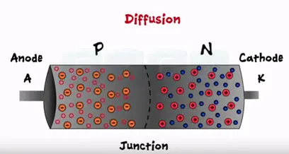
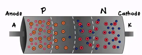
The electron from the N side attracted towards the holes of the P side. These electrons cross over the junction recombine with the holes seem to be free carriers. This process is called diffusion.
The process of recombination continues for sometimes but is restricted near the junction only. As free electrons and holes get depleted from the region near the junction this region is called depletion region.
The depletion contains only negative ions in P side and positive ion in N side of the junction. These ions are immobile.
The motions of electrons do not stop immediately after the formation of depletion region but as they cross the junction. They get repelled by negative ions by P side.
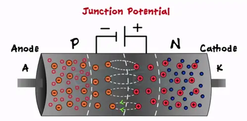
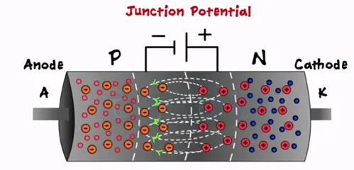
At this point motion of electron stops these charged ions develop electric field in depletion region known as JN potential.
Junction potential is 0.6 volt for silicon and 0.2 volt for germanium. Junction potential restricts electrons crossing the junction further. When external voltage greater than junctional potential is applied to electrons overcome the opposing of junction potential.
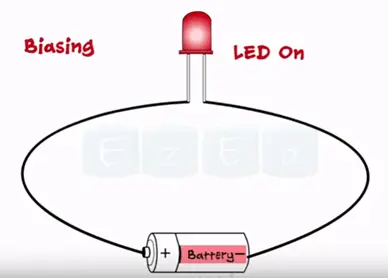
This process of applying external voltage to an electronic device or system to establish suitable working conditions is called as biasing.
The word biasing is used to deplete the inclination or preference towards the particular side. The diode is inclined or biased either in the forward direction or in the reverse direction. Thus diodes are operated in two modes forward and reverse bias.
Forward bias of the diode
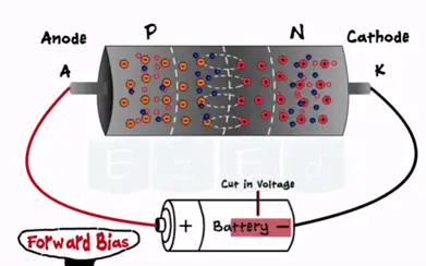
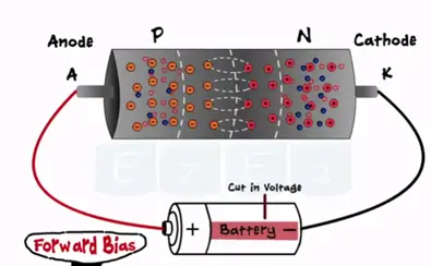
We connect the positive side of the Battery to the anode and negative side to the cathode of the PN junction diode. Internally this positive potential in P side repels the free holes the junction. Negative potential to N side repels free electrons towards the junction.
As we increase the external voltage we applied electrons tried to break the electric field at depletion region and enter into P region. As we increase the voltage over the junction potential value electrons from the N side of the diode attain enough energy to break the electric field and cross over to the other side of the junction.
Thus electron move from the cathode to anode setting up the flow of current from anode to cathode this mode of operation is called forward bias. This current is called drift current.
Reverse bias of the diode
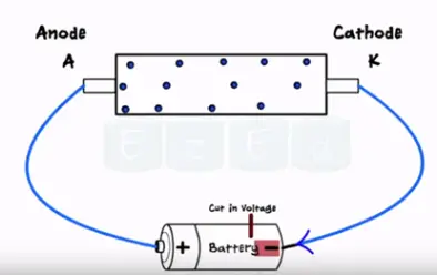
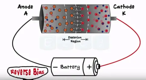
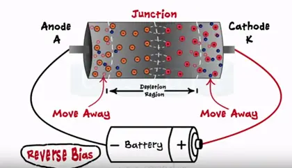
In second case we are applying between in reverse direction. It is negative side of the battery to anode and positive side to cathode. As a result holes are formed to negative of the battery electrons on N side are pull towards positive of the battery. Holes and electrons move away from the junction which leads to increase depletion region.
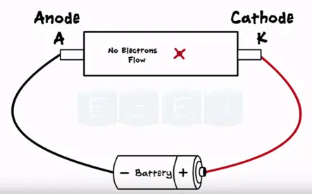
No current flows through the diode. This mode is called reverse bias mode.
But there some minority charge carriers cross always present in both the regions. Hence in the reverse bias minority charge carriers cross the depletion region setting up the current flow. But the magnitude of this current is very low in Nano ampere range.
Ideally in reverse bias current through the diode must be zero. Practically some current flow there as a leakage current

